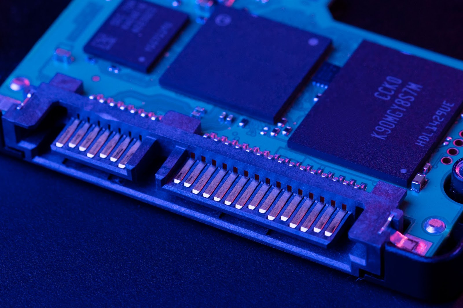
Solid State Drives (SSDs) have transformed the world of data storage with lightning-fast access speeds. At the core, they consist of a printed circuit board festooned with flash memory chips, primarily NAND type. Alongside these memory chips, you’ll find a controller and DRAM memory, crucial components that make the SSD work efficiently.
Core Components of an SSD
- NAND Flash Memory: The primary storage medium for SSDs, these chips retain information and come in various configurations.
- Controller: This microprocessor acts as the brain of the SSD. It manages read and write operations, ensuring efficient data storage and retrieval.
- DRAM Memory: As a cache, the DRAM memory holds frequently accessed data, speeding up the SSD’s performance.
Some advanced SSDs even come with additional memory chips and capacitors, protecting against sudden power failures.
Delving into the Structure of NAND Memory
Writing & Erasing Data:
Writing involves applying a high voltage to the control gate, allowing electrons to populate the floating gate. Erasing data, however, consists in using a reversed voltage setup. But this constant writing and erasing does wear out the dielectric layer over time, limiting the number of times a cell can be overwritten.
Reading Data:
Interestingly, reading doesn’t deteriorate the cell. To discern whether a cell reads a ‘0’ or a ‘1’, voltage is applied, and the current flow is observed. The presence or absence of electrons on the floating gate determines the binary value.
Multi-Level Cells: Storing More Information
Beyond the primary single-level cell (SLC), NAND memory can store multiple bits of information if designed to capture more electrons. For instance, Quad-Level Cells (QLC) can differentiate among 16 threshold voltages to store 4 bits of information. However, reading from QLCs can be slower because of the intricate voltage requirements.
Organizing Cells: Pages & Blocks
To maximize space, NAND memory cells are arrayed in a 3D structure. These cells are grouped to form a 4-kilobyte page—the smallest unit for reading/writing data. Multiple pages combine to create a block, typically 512 kilobytes, the smallest unit that can be erased. This architecture poses certain challenges—overwriting a single page requires erasing and rewriting the entire block. However, the controller manages these operations expertly, ensuring the SSD’s longevity.
The Role of the Controller
A typical SSD controller is a sophisticated piece of hardware. It boasts a 32-bit RISC processor, often with multiple cores, that executes firmware instructions. The controller also interfaces with the DRAM buffer and manages error detection and correction. Furthermore, it ensures data exchanges between memory chips and external interfaces while overseeing encryption and other specific functions.
Connection Interfaces and Form Factors
The speed of an SSD is also influenced by its connection interface. While the 2.5-inch SSDs and mSATA drives often use SATA interfaces, M.2 SSDs could use SATA3 or PCIe, which offers speeds up to 4GB/s depending on its configuration. Other form factors, such as expansion-card SSDs, plug directly into a motherboard’s PCIe slot, boasting even greater speeds.
Conclusion
Solid State Drives have come a long way in their technology and application. Their swift performance, reliability, and evolving technology make them a central element in today’s computing ecosystem. The SSD continues to evolve, offering faster and more efficient storage solutions for consumers and professionals.